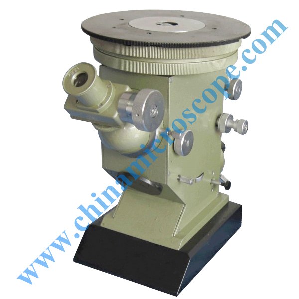
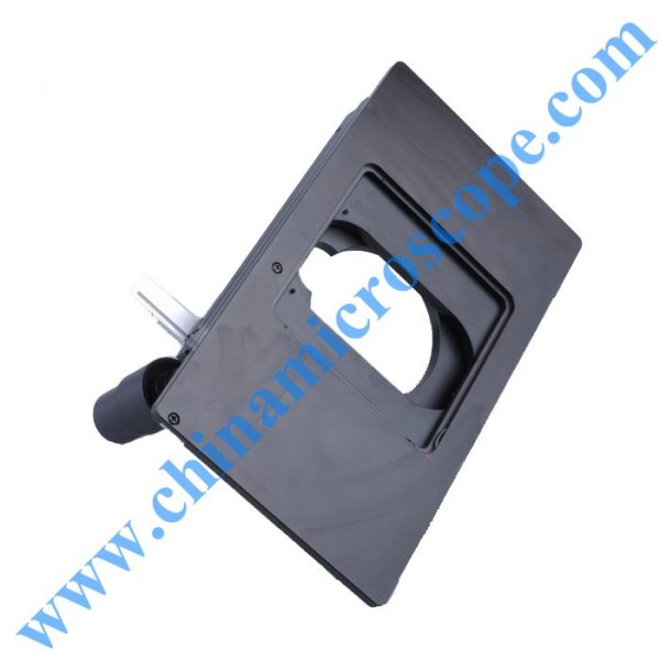
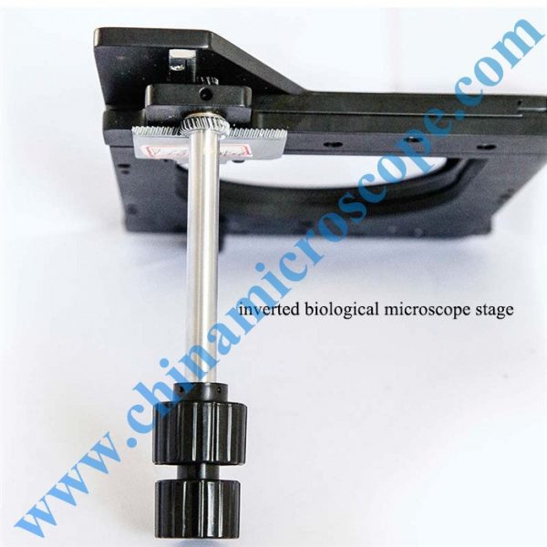
J-M158 Metallurgical microscope is developed and aimed at the semiconductor industry, wafer manufacturing, electronic information industry, metallurgical industry, Used as an advanced Metallurgical microscope, the user can experience its super performance when using it. It can be widely used to identify and analyze Semiconductor, FPD, Circuit encapsulation, circuit substrate, Material, Casting/Metal/Ceramic parts, Precision moulds. This instrument adopts both reflecting and transmitted illumination, Bright&Dark field, DIC and Polarizing observation can proceed under reflecting illumination, and the Bright field observation is done under transmitted light. High quality and reliable optical system brings much clearer and sharper image. The design meets with the ergonomics needs and makes you feel comfortable and relaxed in doing your job.
Characteristics and description
- Adopt UIS High-resolution, long working distance, and infinity light pathcorrecting system objective imaging technology
- Extending the multiplexing technology of objective, compatible infinityobjective with all the observation methods, including bright&dark fieldobservation, polarization and DIC also provide with high clear and sharp image in each observation method.
- Aspherical surface Kohler illumination, increasing the viewing brightness.
- WF10×(Φ25)Super wide viewing field Eyepiece, long working distancemetallurgical objective with bright and dark field
- The Nosepiece can be equipped with detachable DIC differential interferencedevice.


