


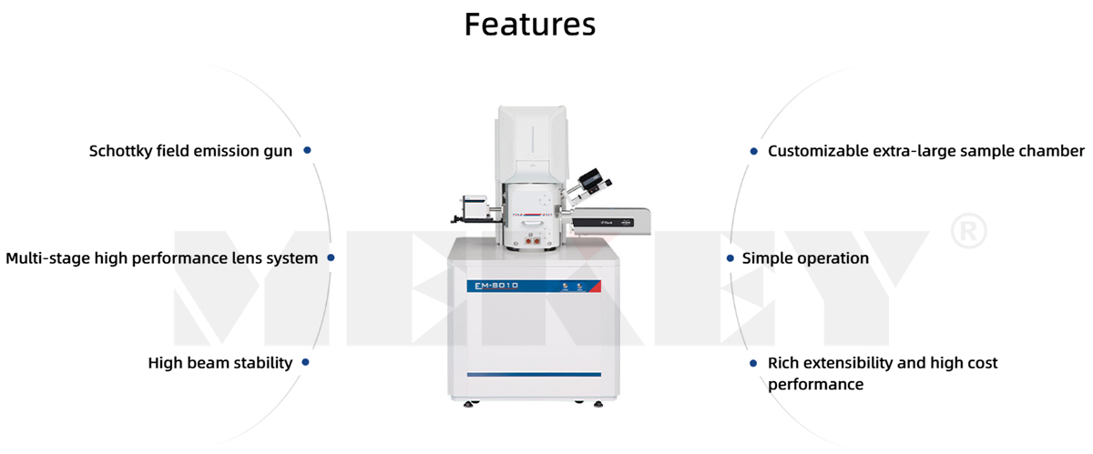
MIC-EM80 series field emission scanning electron microscope is positioned as an economical Schottky thermal field emission scanning electron microscope with rich extensibility and high cost performance, which is widely used in various fields such as materials science, biology, medicine, chemistry, and environmental science.
Field emission gun electron microscope
High resolution field emission scanning electron microscope
Ultra-high resolution field emission scanning electron microscope
FEATURES
Secondary electron detector
High signal-to-noise ratio, high bandwidth
Extended depth of field to characterize the morphology and structure of the sample surface

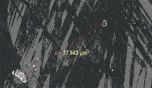
Dimension measurement
With extensive image measurement functions such as distance, angle, horizontal/vertical line, etc
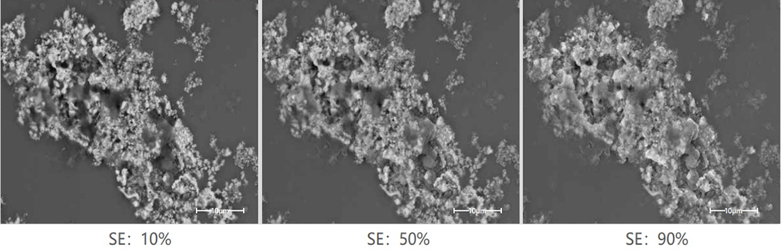
Simultaneous imaging with different detectors
Dual-channel images display of SE and BSESignal mixing ratio of different detectors can be set freely
BSE detector, to detect the composition characterstics of the sample surface

Large image stitching
Continuous automatic image collection
Accurate stitching of multiple images to generate large and high-resolution images

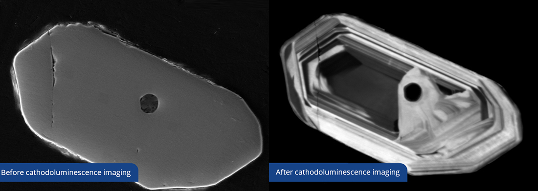
Cathodoluminescence imaging
High signal-to-noise ratio, high band width extended depth of field to characterize the morphology and structure of the sample surface

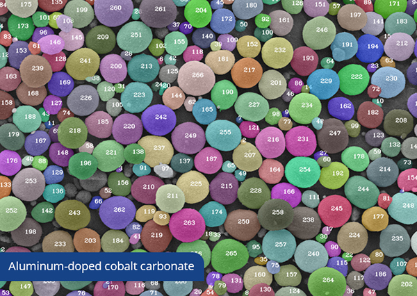
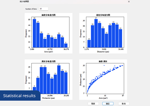
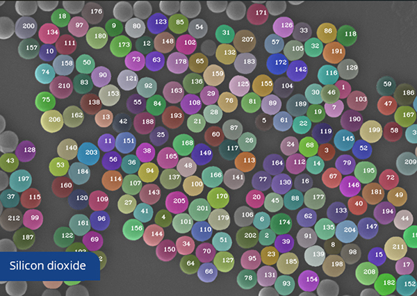
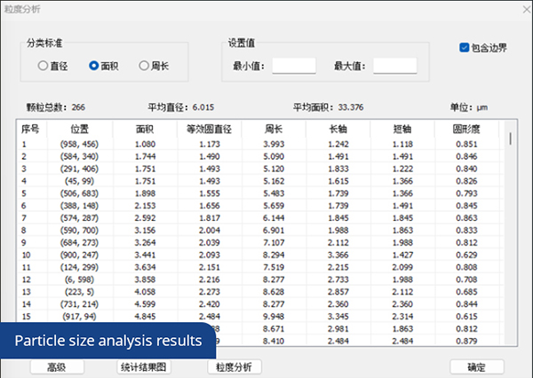
Particle size analysis
The composite image processing algorithm of deep learning is adopted to automatically identify the proportional scale, accurately identify the particles in the image, and count and export various morphological parameters for more comprehensive particle size and particle shape statistics. (Aluminum-doped cobalt carbonate; Silicon dioxide; Statistical results; Particle size analysis results.
Customization
Electron Beam Lithography (EBL)
Functions: The SEM-based electron beam lithography (EBL) system allows precise control of the scanning path and energy deposition of the electron beam to realize high-resolution patterning exposure. The system adopts advanced electron beam scanning control technology, which supports flexible and diverse pattern design and precise control. In addition to the electron beam exposure function, it also retains the original observation function of the SEM, which allows users to complete the observation and processing of samples on the same equipment, improving work efficiency and convenience.
Minimum beam spot better than 5nm; Probe current: 1pA~20nA; Line width better than 15nm
Application Scenarios: Scientific research and teaching; Microelectronics manufacturing; Prototype device development; Nanomaterials preparation; Biomedical research
Processing of 2D periodic array structure
Processing of nano-optical components and microelectronic devices


Vacuum Interconnection
*The vacuum interconnected scanning electron microscope is used for automatic detection of the products transferred by the sample cart, analyze the surface grain morphology, size, distribution and other information, and evaluate the quality of the film.
*The vacuum interconnection system allows the sample to be pre-processed under vacuum and transferred to the scanning electron microscope for observation.
*The automatic detection and feedback system monitors and records sample labels, position status, and sample handover, observing the sample transfer status by CCD or glass window.

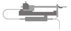
Laser Coupling – Ultrafast Electron Microscope
*The ultrafast electron microscope uses external stimuli such as a laser or electric field to bring the sample to an excited state. Another laser beam with adjustable time delay is applied to the electron microscope filament to generate a pulsed electron beam that irradiates the sample surface, and then collects the secondary electrons escaping from the surface to characterize the excitation transient.

ACCESSORY
EDS-Energy dispersive spectrometer

EBSD-Electron back scattered diffraction
CL-Cathodoluminescence detector
STEM-Scanning transmission electron microscope
Transition chamber
Heating stage

Cooling heading stage

Tensile stage
Specifications
| Item | MIC-EM8010 | MIC-EM8020 |
| High vacuum resolution | SE 1.5nm@15kV BSE 3nm@30kV | |
| Magnification | 1x-600000x
※optical magnification 1x-100x |
1x-600000x
optical magnification 1x-100x |
| Electron gun | Schottky Field Emission Gun | |
| Acceleration Voltage | 0.2kV-30kV | |
| Vacuum system | 2 lon Pumps, 1 Magnetic Levitation Turbo Molecular Pump, 1 Dry Pump | |
| Detector configurations | High vacuum secondary electron detector | High vacuum secondary electron detector |
| Infrared CCD detector | Infrared CCD detector | |
| ※Optical navigation | Optical navigation | |
| ※Four segmentation retractable Back scatter Detector | ※Four segmentation retractable Back scatter Detector | |
| Sample stage | Five axis automatic medium sample stage | Five axis automatic medium sample stage |
| X=80mm | X=150mm | |
| Y=50mm | Y=150mm | |
| Z=30mm | Z=65mm | |
| T=﹣5°~+70° | T=﹣10°~+90° | |
| R=360° | R=360° | |
| Anti-collision alarm function | Anti-collision alarm function | |
| Sample specification | Maximum sample diameter:φ175mm | Maximum sample diameter:φ320mm |
| Maximum sample height: 30mm | Maximum sample height: 90mm | |
| Optional accessory | EDS/EBSD/STEM/CL/Heating stage/Cooling stage/Tensile stage and etc. | EDS/EBSD/STEM/CL/Load lock transition chamber/Heating stage/Cooling stage/Tensile stage and etc. |
※ means optional
Application

Provide customized solutions
Provide you with professional non-standard customized services to meet various application scenarios.


评价
目前还没有评价